MB Turnkey Design LLC
Electronics manufacturer, PCB layouts, RF devices & software

-
General
We are electronics engineering consultants with over 20 years of design and manufacturing experience. Offering unique, hard to find skills and design capabilities in Analog, Digital and RF circuit with complete mechanical design and fabrication capabilities.
Read more -
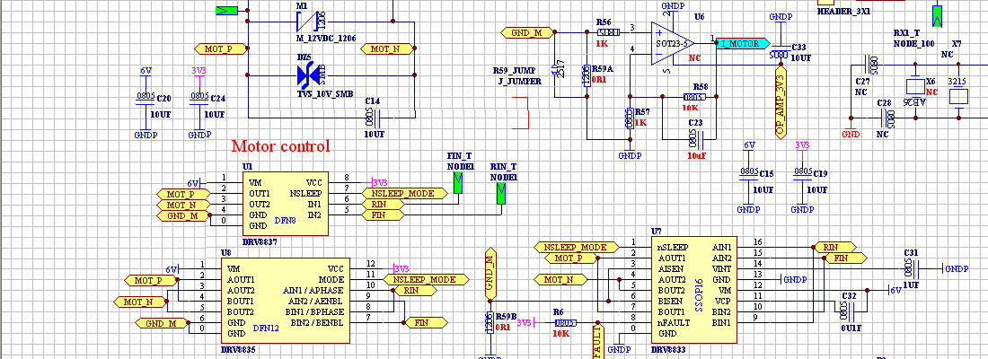
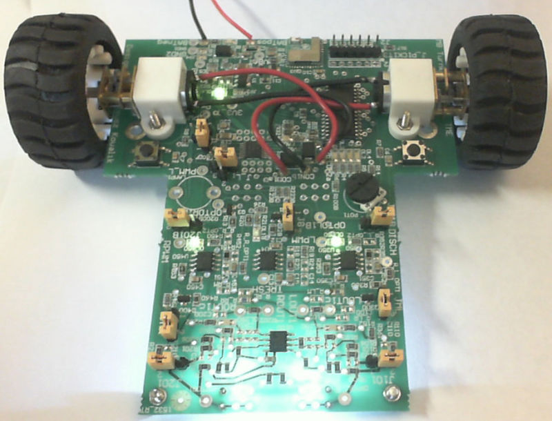
Electronics
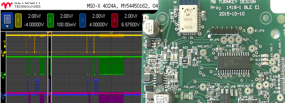
MBTKD offers complete electronic circuit design services including systems integration, data acquisition and motion control for industrial, medical, and commercial applications. We utilizing the latest semiconductor technologies such as RF-wireless, digital computing, FPGA, microprocessors, Bluetooth and discrete power components.
Read more -
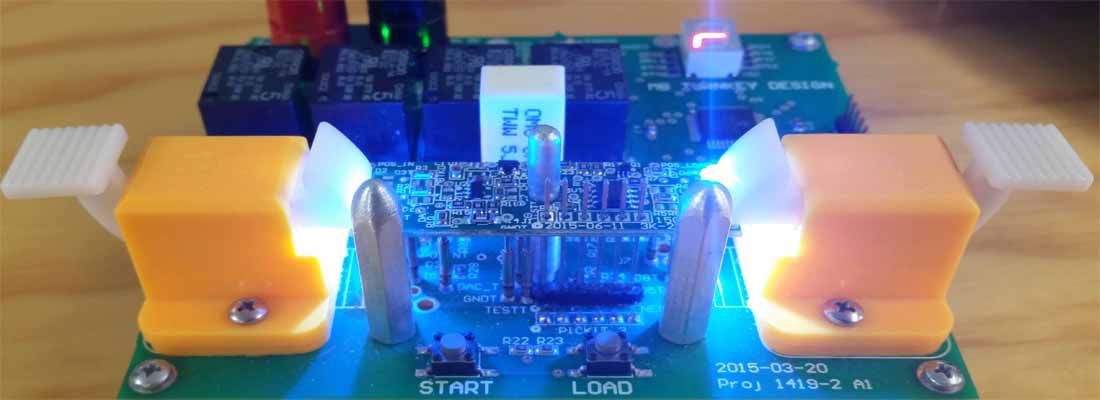
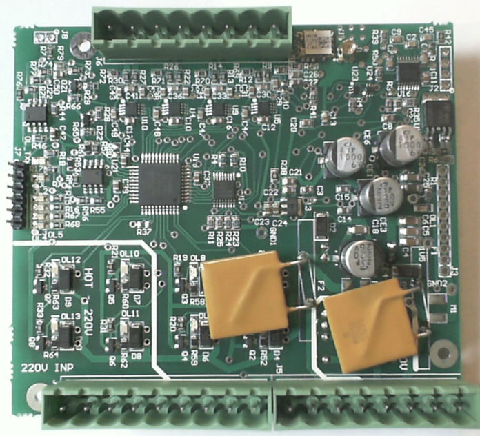
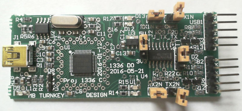
Schematic and PCB design
Our current capabilities include single layer to 12 multi-layer PCB layout design down to 4mils trace width, utilizing SMT and through hole technology with components on one or both sides of the board. MBTKD can also provide rapid prototyping of your existing or new design while reducing overall time to market.
Read more -
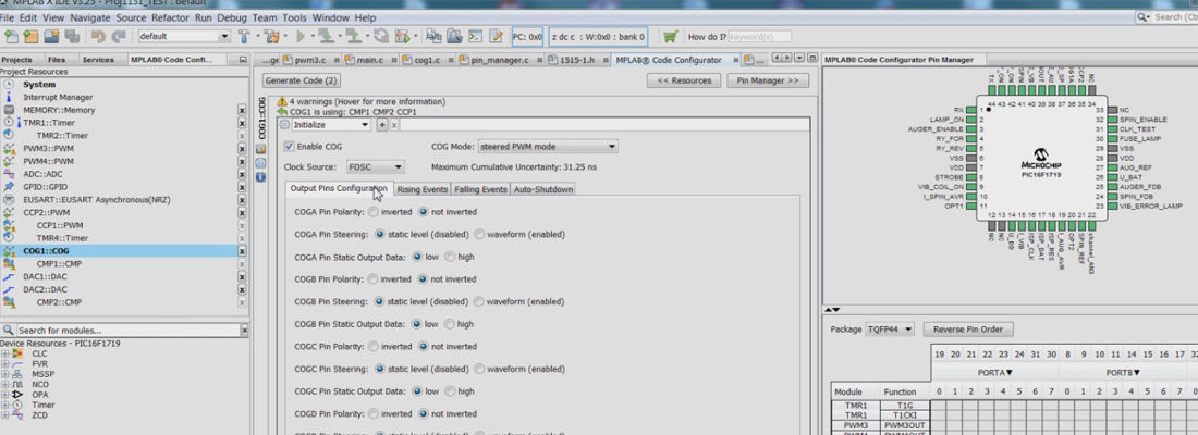
Software
MBTKD offers software design services for embedded computing platforms. Real time operating system (RTOS), C compliers and assembly level programming capabilities as well as full documentation services to complement your hardware designs. .
Read more -
RF Design
MBTKD RF design capabilities include Bluetooth, Zwave mesh networking, short range remotes utilizing a variety of available RF frequency bands compliant with FCC, CE and other agency compliance standards.
Read more -
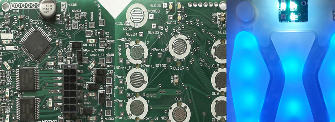
Plastics design
MBTKD addresses all aspects of your visual and physical component design including all of its functions by using Solid Works, a computer aided engineering software to create 3D parametric models. Our current capabilities offer quick concept to finish product fabrication. This results in rapid, cost effective part prototyping by using our on-site 3D printing capability.
Read more -
Smart engineering design
With over 20 years of design and manufacturing experience we will closely work with your firm’s hardware and software requirements. Whether your application is automotive, industrial, medical or commercial it will be under consistent review it to produce the most reliable and cost effective solution.
Read more -
Free quote
Our contract engineering group can provide a free quote for implementation of Automation Procedures and Techniques for your Electronic Design, RF Remote Control Design and Plastic Design.
Read more -
Free project review
We will meet with you to review your all of your project requirements and provide free initial consulting regarding any one of your Automation Techniques, Electronic Design, Plastic Design and RF Remote Control Design..
Read more -
Domestic production
Our New Jersey facility offers rapid prototyping and low and high volume production to meet demanding time-to-market schedules by using the latest CAD/CAM tools to ensure the highest quality products in the shortest time possible.
Read more -
Offshore production
High volume applications can be manufactured with one of our off-shore partners that can provide complete assemblies that are fully tested and documented to your specifications.
Read more -
Quality Guarantee
We guarantee all of our products and services which is easy with the by using the standards of UL, CSA, FCC and other regulatory commissions.
Read more
Recent projects
Portfolio block allows you to show your projects or products right on the homepage.
Testimonials
More opinionsIt is uncommon to find the level of support you have given us in training and support for the few repairs required on this old equipment. You are very innovative and stand by you innovations to make sure they are trouble free for years.
Gerry
My experience with MB Turnkey Design is that when they commit themselves to a project they will deliver the full engineering services required to assure the quality, documentation and working prototypes on time.
Jim Fair
I look forward to continued success inour ongoing business as well a new developments and future projects. Please stay well and stay in touch.
Kenneth Krawcheck
About us
MB Turnkey Design specializes in designing with Microchip products. Visit the Microchip Technology website for more information by clicking here.
![[X]](img/x.png)